CHIP-48: Technical Reference #
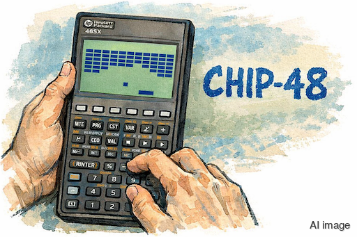
(A compact, implementation-level description of CHIP-48, suitable for both program authors and emulator writers that want to implement it as its own CHIP-8 variant instead of as a collection of quirks.)
You know CHIP-8 and are only interested in a compact description of the differences? Jump to the TLDR section.
1 Overview #
CHIP-48 is a CHIP-8 variant for a calculator implementation. It keeps the small 4k address space and the 64×32 two-color CHIP-8 screen, but adapts timing, display handling, and a few instructions to that platform.
It defines a virtual machine with:
- 4kB of addressable memory (
0x000-0xFFF). - Sixteen 8-bit general-purpose registers
V0...VF. - One 16-bit index register
Ias an index into the ram. - Two 8-bit timers (
DT, the delay timer,STthe sound timer) that count down at 64Hz. - A two-color 64×32 pixel interpreter display.
- A hexadecimal keypad with 16 keys (0-F).
- A buzzer controlled by the sound timer.
All CHIP-48 programs are loaded at memory location 0x200, where the interpreter begins execution
after a reset.
2 Virtual Machine Model #
2.1 State #
For the definition of the state, the following table uses the types:
uint8= 8-bit unsigned integeruint16= 16-bit unsigned integer
Choose the types that match this best for your chosen language.
The CHIP-48 VM/interpreter has the following state:
| Name | Type | Description |
|---|---|---|
V0...VF | array of 16 uint8 | General-purpose data registers. VF also acts as a flag register (carry/borrow/pixel-collision); if there’s a conflict between using VF as a normal register vs. as a flag, the flag meaning wins. |
I | uint16 | Index / memory address register (used e.g. for sprite addresses, BCD conversion, etc.). |
DT | uint8 | Delay timer; decremented at 64 Hz while non-zero. |
ST | uint8 | Sound timer; decremented at 64 Hz while non-zero; a beep is produced while ST > 0. |
PC | uint16 | Program Counter; starts at 0x200. Normally increments by 2 per fetched instruction; some instructions change it further. |
SP | uint16 | Stack pointer; points to the top of the call stack. |
stack | array of 16 uint16 | Call stack storage, commonly modeled as an array with at least 16 entries. |
ram | array of 4096 uint8 | Main memory: 4k of RAM, organized in bytes. |
screen | array of 2048 uint8 | Display buffer for the 64×32 CHIP-48 interpreter screen. A byte per pixel is the easiest generic representation, even if the calculator displays each interpreter pixel as a 2×2 block of LCD pixels. |
Stack pointer SP and program counter PC are internal registers of the interpreter, and in-accessible to
a CHIP-48 program. The model suggested here is the most common approach to implement them, but stack could
also be a stack-container if the chosen language offers one, and in that case the stack pointer would be omitted
(it’s the size of the container). The program counter could also be a pointer into the ram or an iterator.
2.2 Memory Layout #
A generic CHIP-48 implementation has 4k ram organized in bytes with a memory layout like this:
0x000-0x04F   built-in CHIP-48 font
0x050-0x1FF   unused
0x200-0xFFF   Program / working RAM
The largest practical CHIP-48 program size is 3583 bytes. The range from 0x200 to 0xFFF
contains 3584 bytes, but a program actually using all of them would make the interpreter crash.
As in all CHIP-8 variants of the knowledge base, the execution range of the program is limited to 0xFFF, as
all instructions allowing to influence the program counter are limited to 12 bit parameters.
2.3 Timers #
- Both timers are unsigned 8-bit counters.
- When set to a non-zero value they decrement automatically at 64 Hz, synced to the calculator frame rate.
2.4 Sound #
For generic CHIP-48 the sound timer enables a simple sound output. Sound is active while ST > 0, and as
implementor of a CHIP-48 interpreter you can freely decide on a pitch or waveform to your liking.
Be aware to decrement the timers ideally at the start of the video frame and not right after the opcode execution of a frame, as then the delay or buzzing will be shorter by one frame. Delays or beeps of length 1 will even have no effect, and setting delay to 1 is a very common pattern to pace a game.
2.5 Graphics #
| Property | Value |
|---|---|
| Resolution | 64×32 interpreter pixels |
| Colour depth | Monochrome (pixel = on/off) |
| Drawing mode | XOR - sprites are XORed onto the current framebuffer. If any pixel changes from set to unset during a Dxyn, set VF = 1, and if that happens not once during the drawing set VF = 0. |
| Refresh | 64Hz as used by the calculator implementation. |
The physical calculator display is 131×64 pixels. The CHIP-48 interpreter screen is still only 64×32 pixels, and the calculator draws each interpreter pixel as a 2×2 block of LCD pixels. Generic CHIP-48 emulation does not need to expose that physical detail, and can simply present the logical 64×32 screen.
CHIP-48 has a display wait. A generic interpreter should break out of the frame execution loop after a Dxyn
instruction, so at most one draw instruction is executed per frame.
2.6 Font Set #
The regular font data is at address 0x0000 and consists of 16 sprites for the hexadecimal digits 0-F.
It’s made up of these 16 characters:
The data for easy use in an emulator:
    0xF0, 0x90, 0x90, 0x90, 0xF0,  // 0
    0x20, 0x60, 0x20, 0x20, 0x70,  // 1
    0xF0, 0x10, 0xF0, 0x80, 0xF0,  // 2
    0xF0, 0x10, 0xF0, 0x10, 0xF0,  // 3
    0x90, 0x90, 0xF0, 0x10, 0x10,  // 4
    0xF0, 0x80, 0xF0, 0x10, 0xF0,  // 5
    0xF0, 0x80, 0xF0, 0x90, 0xF0,  // 6
    0xF0, 0x10, 0x20, 0x40, 0x40,  // 7
    0xF0, 0x90, 0xF0, 0x90, 0xF0,  // 8
    0xF0, 0x90, 0xF0, 0x10, 0xF0,  // 9
    0xF0, 0x90, 0xF0, 0x90, 0x90,  // A
    0xE0, 0x90, 0xE0, 0x90, 0xE0,  // B
    0xF0, 0x80, 0x80, 0x80, 0xF0,  // C
    0xE0, 0x90, 0x90, 0x90, 0xE0,  // D
    0xF0, 0x80, 0xF0, 0x80, 0xF0,  // E
    0xF0, 0x80, 0xF0, 0x80, 0x80   // F
NOTE:
Load the font into memory on every reset (as the previous program run could have modified it).
2.7 Input (Hex Keypad) #
The keypad consists of 16 keys labeled 0-F. Key states are queried by opcodes Ex9E, ExA1, and Fx0A.
The opcodes Ex9E, ExA1, and Fx29 only use the lower 4 bits of Vx. So a value greater than 15 is not
an error here, the upper 4 bits are ignored.
3 Instruction Format #
- All instructions are 16 bit (2 bytes), stored big-endian (
high bytefirst). - The most significant nibble determines the primary opcode class; the remaining nibbles supply operands or further opcode distinction.
For this reference the naming convention is following the one used in the original CHIP-8 documentation, but using lowercase letters for better distinction from the opcode defining nibbles:
| Symbol | Meaning |
|---|---|
n | 4-bit value (0-F) |
kk | 8-bit immediate |
mmm | 12-bit address |
x, y | Register indices (0-F) |
After fetch, the PC normally is incremented by 2 and jump-, branch-, or skip-instructions modify it explicitly.
4 CHIP-48 Opcode Set #
The table below enumerates the CHIP-48 opcode set. Opcodes not mentioned as different behave like classic CHIP-8.
| Opcode | Description |
|---|---|
00E0 | clears the screen |
00EE | return from subroutine to address pulled from stack |
0mmm | native machine-code call in classic CHIP-8; for a generic CHIP-48 emulator this can be ignored or treated as invalid |
1mmm | jump to address mmm |
2mmm | push return address onto stack and call subroutine at address mmm |
3xkk | skip next opcode if Vx == kk |
4xkk | skip next opcode if Vx != kk |
5xy0 | skip next opcode if Vx == Vy |
6xkk | set Vx to kk |
7xkk | add kk to Vx (no flag is set on overflow) |
8xy0 | set Vx to the value of Vy |
8xy1 | set Vx to the result of bitwise Vx OR Vy; VF is left unchanged |
8xy2 | set Vx to the result of bitwise Vx AND Vy; VF is left unchanged |
8xy3 | set Vx to the result of bitwise Vx XOR Vy; VF is left unchanged |
8xy4 | add Vy to Vx, VF is set to 1 if an overflow happened, to 0 if not, even if x=F! (VF is written last) |
8xy5 | subtract Vy from Vx, VF is set to 0 if an underflow happened, to 1 if not, even if x=F! (VF is written last) |
8xy6 | shift Vx one bit to the right, set VF to the bit shifted out; y is ignored |
8xy7 | set Vx to the result of subtracting Vx from Vy, VF is set to 0 if an underflow happened, to 1 if not, even if x=F! (VF is written last) |
8xyE | shift Vx one bit to the left, set VF to the bit shifted out; y is ignored |
9xy0 | skip next opcode if Vx != Vy |
Ammm | set I to mmm |
Bxkk | jump to address xkk + Vx, so the x nibble doubles as the upper address nibble and the index of the register to add |
Cxkk | set Vx to a random byte masked (bitwise AND) with kk |
Dxyn | draw 8×n pixel graphics at position Vx & 63, Vy & 31 with data from memory, starting at the address in I, I is not changed; display wait applies |
Ex9E | skip next opcode if key in the lower 4 bits of Vx is pressed |
ExA1 | skip next opcode if key in the lower 4 bits of Vx is not pressed |
Fx07 | set Vx to the current value of the delay timer |
Fx0A | wait for a pressed key to be released and set Vx to its number |
Fx15 | set delay timer to Vx |
Fx18 | set the sound timer to Vx, the buzzer is buzzing until the sound timer is back to 0, setting it to 0 stops an ongoing buzz |
Fx1E | add Vx to I; if this increments I above 0xFFF, the interpreter ends |
Fx29 | set I to the 5 line high hex graphics for the lowest nibble in Vx, using the font at 0x0000 |
Fx33 | write the value of Vx as BCD value to memory at the addresses I (hundreds), I+1 (tens) and I+2 (ones) |
Fx55 | write the content of V0 to Vx at the memory pointed to by I, I is incremented by x |
Fx65 | read the bytes from memory pointed to by I into the registers V0 to Vx, I is incremented by x |
NOTE:
The8xy1/8xy2/8xy3instructions are a visible difference to classic CHIP-8 because they do not clearVF. Also be aware that8xy6and8xyEare Vx-only shifts here, so theynibble is ignored.
5 Main Loop / Execution Cycle #
A generic CHIP-48 emulator should follow the following main loop:
- handle inputs
- decrement timers (if not 0)
- execute IPF (that is Instructions Per Frame) instructions in an inner loop
- Fetch two consecutive bytes from memory at the address in
PC, incrementingPCby 2 - Decode often using the most significant nibble for an initial switch and further if statements or nested switches for the instruction not fully specified by one nibble
- Execute the instruction, updating registers, memory, display, timers, or PC as required
- Break out of the inner loop after
Dxyn, because CHIP-48 has display wait
- Fetch two consecutive bytes from memory at the address in
- update the displayed ui screen with the new content
- wait for the rest of the frame time to run at 64Hz
An adequate speed is 15 instructions per frame. At 64Hz this means that the interpreter executes about 960 instructions per second, besides the limiting effect of display wait.
6 Reset Sequence & Program Loading #
The recommended initialization and loading of programs is as follows:
- Clear memory (all bytes set to
0) - Copy the CHIP-48 font into memory at offset
0x000 PC = 0x200I = 0- All
Vx = 0 DT, ST = 0- Clear screen (all pixels off)
- Binary image of CHIP-48 program is copied/loaded into memory starting at
0x200.
The actual order of these steps is flexible, as long as you keep memory clearing in front of the font initialization and program loading.
7 CHIP-48 Quirks #
Compared to classic CHIP-8, CHIP-48 is often the source of what later gets implemented as configurable “quirks” in generic emulators. For a CHIP-48 mode, these are not optional quirks though, but part of the variant:
- Timer rate - timers and frames run at 64Hz, not 60Hz.
- Execution speed - 15 instructions per frame is an adequate default.
- Display wait - stop the instruction loop for the frame after
Dxyn. - Bit operations (
8xy1,8xy2,8xy3) -VFis left unchanged. - Shift instructions (
8xy6,8xyE) - the source and destination register is Vx, andyis ignored. - Offsetted jump instructions (
Bxkk) - jumps toxkk + Vx, not tommm + V0. - Index overflow (
Fx1E) - incrementingIabove0xFFFends the interpreter. - Register load and store (
Fx55,Fx65) -Iis incremented byx, not byx+1.
TLDR: What is Different to CHIP-8? #
Okay, you know CHIP-8, but what’s different about CHIP-48? Here are the differences collected at one place:
- Memory is 4k as on CHIP-8, but allows for 3583 bytes as the max size of a program (theoretically 3584 should fit, but it would crash).
- Framerate is 64 Hz instead of 60 Hz.
- An adequate IPF rate is 15 instructions per frame.
- The display of the calculator is 131×64 pixels, so the 64×32 display of the interpreter screen is drawn as 2×2 LCD pixels per CHIP-8 pixel
- There is a display wait.
8xy1/8xy2/8xy3do not resetVFbut leave it unchanged.8xy6/8xyEare only useVx, so they doVx >>= 1/Vx <<= 1instead ofVx = Vy >> 1/Vx = Vy << 1andyis ignored.Bmmmhere isBxkkand jumps toxkk + Vx, so thexnibble doubles as part of the 12 bit address and an index for the register to add.- Incrementing
Iabove0xFFFwithFx1Eends the interpreter. Fx55/Fx65incrementIbyxinstead ofx+1.
Generic CHIP-48 emulation does not need to render the screen in 2x2 pixels, it is just an artifact of the calculator platform.
Regular Font Data (4x5) #
The font of CHIP-48 is at address 0x0000 and made of this patterns:
It’s made up of these 16 characters:
The data for easy use in an emulator:
    0xF0, 0x90, 0x90, 0x90, 0xF0,  // 0
    0x20, 0x60, 0x20, 0x20, 0x70,  // 1
    0xF0, 0x10, 0xF0, 0x80, 0xF0,  // 2
    0xF0, 0x10, 0xF0, 0x10, 0xF0,  // 3
    0x90, 0x90, 0xF0, 0x10, 0x10,  // 4
    0xF0, 0x80, 0xF0, 0x10, 0xF0,  // 5
    0xF0, 0x80, 0xF0, 0x90, 0xF0,  // 6
    0xF0, 0x10, 0x20, 0x40, 0x40,  // 7
    0xF0, 0x90, 0xF0, 0x90, 0xF0,  // 8
    0xF0, 0x90, 0xF0, 0x10, 0xF0,  // 9
    0xF0, 0x90, 0xF0, 0x90, 0x90,  // A
    0xE0, 0x90, 0xE0, 0x90, 0xE0,  // B
    0xF0, 0x80, 0x80, 0x80, 0xF0,  // C
    0xE0, 0x90, 0x90, 0x90, 0xE0,  // D
    0xF0, 0x80, 0xF0, 0x80, 0xF0,  // E
    0xF0, 0x80, 0xF0, 0x80, 0x80   // F